Page 188 - 《摩擦学学报》2021年第5期
P. 188

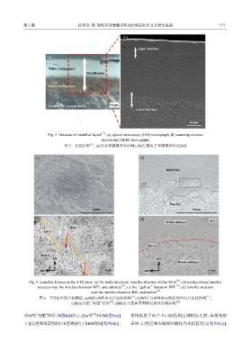
第 5 期                     沈明学, 等: 轮轨界面摩擦学转变结构层特性及其研究进展                                       777


                                                            (b)

                                                                  Upper interface
                       (a)


                        White etching layer
                                          Stratification


                        Brown etching layer


                        Pearlite (P) = parent matrix  10 μm
                                                                 Lower interface


                                                                                           10 μm


                                                 [17]
                        Fig. 3  Structure of stratified layers : (a) optical microscopy (OM) micrograph, (b) scanning electron
                                                 microscopy (SEM) micrograph.
                                            [17]
                                图 3    分层结构 : (a)光学显微镜图片(OM),(b)扫描电子显微镜图片(SEM)
                  (a)                                              (b)


                                                                                Rail WEL


                                                                                  Pearlite
                                             2 μm                                           10 μm

                  (c)                                              (d)
                                                                                White sublayer      Al-1
                                  BEL
                      Int-1


                                                                       Int-1a

                    Matrix
                          ND                                               ND
                                                                                     Brown sublayer

                    RD                             1 μm              RD                             1 μm

                                                                                     [31]
               Fig. 4  Lamellar features in the TTS layer: (a) the multidirectional lamellar structure within WEL ; (b) unidirectional lamellar
                                                           [31]                     [18]
                   structure near the interface between WEL and substrate ; (c) the “gullies” feature in BEL ; (d) lamellar structure
                                                                           [18]
                                            near the interface between BEL and matrix
                    图 4    TTS层中的片状特征:(a)WEL内的多向片层状结构 ;(b)WEL与基体界面附近的单向片层状结构 ;
                                                               [31]
                                                                                                   [31]
                                   (c)BEL内的“沟壑”特征 ;(d)BEL与基体界面附近的片层状结构               [18]
                                                     [18]
                                             [32]
            明显的“沟壑”特征,如图4(d)所示. Zhu等 对OM[图5(a)]                发现低倍下两个不同颜色的区域均较光滑,高倍观察
            下呈白色和淡黄色的TTS区域进行了SEM观察[见图5(b)],                    表明:白色区域内微观结构较为光滑且均匀[见图5(c)],
   183   184   185   186   187   188   189   190   191   192   193